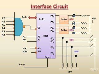
10+ 8255 block diagram
8255 PPI contains 24 programmable IO pins arranged as 2 8-bit ports 2 4-bit ports. Programmable Peripheral Interface Block Diagram.

2019 2 3l Ecoboost Water Pump Housing Part Number Ford Mustang Ecoboost Forum
It has three separately accessible ports.
. These are 8 -bit bi-directional buses connected to 8085 data bus for transferring data. It has 24 inputoutput lines which may be individually programmed in two groups of twelve. 8255 PPI contains 3 ports and they are arranged in two groups of 12 pins.
A B and C The individual ports can be programmed. The 8255 Programmable Peripheral Interface PPI It is one of the most widely used IO chips. Data busD 0 -D 7.
The Intels 8255 is designed for use with Intels 8-bit 16-bit and higher capability microprocessors. Describe the Block diagram of 8255. Solve only Part B a Draw a block diagram of a microprocessor based system interfaced with 8255 8254 8259 8237and RAMAlso show clock generator buffers transceivers and address.

8255 Programming
2

Semi Truck Anatomy Google Search Cosas De Coche Libros De Mecanica Automotriz Mecanica Automotriz
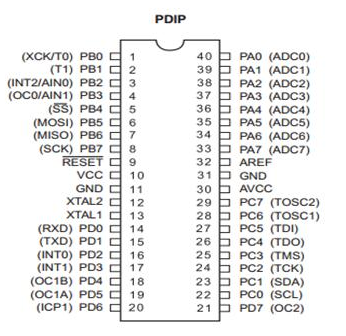
Atmega32 Pin Diagram Javatpoint
Atmega32 Pin Diagram Javatpoint

8255 Programming
2

8255 Programming
What Is What If Analysis In Microsoft Excel Quora

8255 Programming
8255 Programming
Lacan S Graph Of Desire Sticker For Sale By Acidhorizon Redbubble

Motorola 6800 Wikiwand
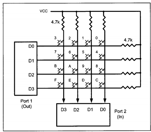
Keyboard Interfacing With Avr Javatpoint
8255 Programming

8255 Programming

Qfp64 0 5 Rev2 Adapter